
How Two Companies Control the World’s Most Valuable Resource
The Ultimate “Forever Stocks” for Today’s Computing Revolution
| Welcome to Porter & Co.! If you’re new here, thank you for joining us… and we look forward to getting to know you better. You can email Lance, our Director of Customer Care, at this address, with any questions you might have about your subscription… The Big Secret on Wall Street… how to navigate our website… or anything else. You can also email our “Mailbag” address at: [email protected]. Paid subscribers can also access this issue as a PDF on the “Issues & Updates” page here. |
For the next three weeks in The Big Secret on Wall Street (through June 28), we’ll continue our exploration of the extraordinary investment series we launched last week. It’s the next step of the technological revolution… it involves (and goes far beyond) artificial intelligence and machine learning… and right now, no one is talking about it like we are.
In honor of Porter & Co.’s second anniversary, we’re making this vital four-part series free to all our readers. You’ll get the high-level view of this tech revolution and receive a number of valuable investment ideas along the way. However, detailed recommendations and portfolio updates will be reserved for our paid subscribers. If you are not already a subscriber to The Big Secret on Wall Street, click here…
We call this big story The Parallel Processing Revolution, and we’re thrilled to share the second part of it with you today.
Crash!
On a micro scale, it could have been the sound of nuclear fission at the heart of an atomic weapon.
On the streets of Albuquerque one December day in 1945, it was the sound of two inept young spies bumping into each other.
Nineteen-year-old Ted Hall and 20-year-old Saville Sax, two young Communist-leaning Americans, had accepted a dangerous assignment from the Soviet Union… steal the plans for America’s top-secret nuclear bomb, code-named the Manhattan Project.
After four years of development at classified locations in the U.S. and England, the bomb was nearly complete, ready to deliver the final blow to the faltering Axis powers at the end of World War II.
And Soviet dictator Joseph Stalin felt a little left out.
Though Russia was allied with America and Britain, the two Western nations didn’t trust the Union of Soviet Socialist Republics quite enough to share their atomic secrets. But “Uncle Joe” Stalin wanted a nuclear bomb for Mother Russia… and what Stalin wanted, he usually got.
So as American and British scientists fine-tuned the fission and fusion of the atom, the Soviets infiltrated the Manhattan Project labs with a ring of carefully selected informants… known today as the “atomic spies.”
Ted, a Harvard graduate by 18, and the youngest physicist working on the bomb, was an obvious target for the Soviets. He’d put on what he called “pink-colored glasses” during his time at college, and believed nuclear weaponry should be shared equally with all.
Ted had something extra valuable to share with Russia: he’d personally designed the central combustion mechanism of the “Fat Man” plutonium bomb that would soon destroy Nagasaki, Japan.
As the informant, Ted (code-named “Young”) passed critical intel to Saville, the courier (code-named “Old”), who then headed back to the spies’ Russian handler in New York.
Ted was young indeed. And his idea of espionage came straight out of the funny papers.
No one saw Ted approach the Albuquerque meetup from the wrong direction and smash into his contact… or the cartoon-style handoff where Saville stuffed the blueprint for “Fat Man” into his shoe.
Though the handoff wasn’t a masterclass in spycraft, the traitorous teen still single-handedly gifted the Russians their own nuclear weapon. In 1949, the Soviets tested their first homegrown plutonium bomb… using the same groundbreaking design that Ted had slipped to Saville.
Ultimately, Ted also gave the world the gift of the Cold War, where America and Russia spied on each other obsessively and amassed ever-growing piles of deadly nuclear technology during the protracted middle part of the last century.
In an interview with The New York Times in 1997, a 71-year-old Ted Hall suggested that he’d changed the course of history. And he was, by and large, proud that he’d stopped American nuclear monopoly in its tracks. “Maybe the ‘course of history,’ if unchanged, could have led to atomic war in the past 50 years – for example the bomb might have been dropped on China in 1949 or the early 50’s,” he said. “Well, if I helped to prevent that, I accept the charge.”
Where there are secrets, there are always spies. Carefully guarded inventions invariably spark competition and chicanery. And whenever one group monopolizes a game-changing technology, some kind of arms race is sure to follow.
Human civilization is built of space races, arms races, oil races – a never-ending cycle of cold and hot wars as superpowers fight for limited resources. In the early decades of the 21st century, in addition to our perennial global tug of war over weapons and energy, we’ve added a new conflict into the mix: the chip race.
Complete with its own tight monopolies and industrial spies, this new arms race centers on the global battle to control advanced semiconductors, known as sub-10 nanometer (“nm”) chips. These tiny slivers of metal – and the factories that build them – are the cornerstone of the global economy, powering everything from smartphones to data centers to missile guidance systems, not to mention the accelerating artificial-intelligence (“AI”) industry.
Remarkably (and similar to the American-British chokehold on nuclear technology during the 1940s), the supply chain for the massive semiconductor industry – which generates about $600 billion in revenue per year – rests in the hands of just two companies… making the rest of the world almost totally dependent on them.
Neither of these companies are in China. And oh boy, do the Chinese want a piece of them…
Last year, China spent $390 billion importing semiconductor chips and manufacturing equipment – 15% more than what it spent importing oil. Right now, China manufactures a few chips of its own, but none of the most advanced variety. So it’s scrambling madly to beg, borrow, and steal intellectual property (“IP”) from chipmakers around the world… particularly, the two companies with the virtual chip monopoly.
Not surprisingly, China currently has its own semiconductor version of atomic spies – and at least one of them got off scot-free.
Mutually Assured Dinero
Of the hundreds of Communist sympathizers in the U.S. who were Soviet informants during the Manhattan Project, only a few, very high-profile spies were ever tried and convicted. Klaus Fuchs, a high-level turncoat scientist, got nine years in jail, and Julius and Ethel Rosenberg notoriously received the death penalty for “conspiracy to commit espionage” in 1953.
Declassified Russian documents show that countless code-named others slipped away: “Fogel,” “Mar,” “Quantum,” “Eric.” Melita Norwood, an unassuming secretary who filched bomb blueprints throughout her 40-year career and only fessed up after her retirement. And, of course, Ted Hall (“Young”) – whose real name (presumably accidentally) appeared once in his Soviet handlers’ files.
Ted was questioned by U.S. government authorities a few times during the war, but was never apprehended – and he went on to get married and live an unremarkable life as a researcher in biophysics, granting a few cagy interviews toward the end of his life. The most he ever outright admitted to was being “worried about the dangers of an American monopoly of atomic weapons.”
It seems that Chinese engineer Zongchang Yu has managed so far to wriggle through the net in much the same way.
Yu weaseled his way into a top spot at one of the two companies that controls the chip industry – and then left the company in 2012, taking a sizable chunk of its proprietary software with him. Two years later, Yu launched Dongfang, a now-successful Beijing-based semiconductor company.
There’s still a warrant out for Yu’s arrest in his former adopted state of California on a count of intellectual property theft… but the Santa Clara County sheriff is unlikely to find him behind the Bamboo Curtain. No doubt, like Ted, Yu is “worried about a monopoly” on semiconductor chips.
To be fair, China is not the only country trying to snatch a helping of chips. Neither of the monopolizing companies is American – so, in order to keep up, America is pouring billions of dollars into developing its own semiconductor industry.
In August 2022, Congress passed and President Joe Biden signed the cleverly-named CHIPS Act (Creating Helpful Incentives to Produce Semiconductors). This act – the largest-ever domestic infrastructure bill aimed at a single industry – authorizes roughly $280 billion to fund research and manufacturing capacity for domestic semiconductor production in the U.S. This government funding, along with tens of billions from the private sector, aims to reverse a four-decade long trend of U.S. chipmakers outsourcing production.
However, as we’ll show in this issue, despite the flood of Chinese and American investment dollars and blatant Chinese IP theft, neither country has succeeded in displacing the two choke points in the global chip-production supply chain.
The reason: these companies control the most sophisticated manufacturing operations in human history. They maintain such a powerful, entrenched advantage over the rest of the industry that the best efforts of the two largest governments in the world have failed to replicate them.
And all evidence suggests that these two firms will continue to dominate the global semiconductor supply chain for years to come. These companies – which, although they are not headquartered in the U.S., are publicly traded on the Nasdaq and NYSE – are the two best ways for investors to capitalize on today’s parallel-processing revolution.
To bastardize another arms race term, it’s mutually assured dinero.
Let’s get started with the largest monopoly of them all – the company with 100% market-share dominance in the critical machines used to make today’s most advanced semiconductors.
Leaving Moore’s Law in the Dust
Founded in the Netherlands in 1984, ASML (Nasdaq: ASML) is the global leader in photolithography machines used in semiconductor manufacturing. With a market cap of $424 billion, it generated $28 billion in revenue in 2023, a 29% increase over 2022.
Photolithography machines use light energy to etch intricate patterns onto the silicon wafers of semiconductors. These patterns enable the precise placement of components onto computer chips – including transistors, the key building block of electronic devices.
First, though, a bit of background on transistors and their critical role in driving advancements in computing power…
Transistors exist in one of two states: on or off, depending on the flow of electricity through a computer chip. This on/off state translates into a 0 or 1, which forms the basis of the binary code instructions in all computer-programming languages.
The more transistors on a computer chip, the more binary code it can process, and thus the greater its computing power.
As we wrote last week, the co-founder of U.S. chipmaker Intel, Gordon Moore, noticed in the 1970s that the number of transistors going into cutting-edge microprocessors was doubling every 18 to 24 months – and so the processing speed was increasing at similar rates. The observation became known as Moore’s Law, and the advancements in computer processing speeds has largely followed this projection over the last five decades. This exponential increase in computing power has made modern-day life possible.
While chipmakers get much of the credit for engineering and manufacturing ever-more advanced semiconductors, none of this progress would exist without the advancements in photolithography equipment. By finding new ways to etch smaller, more precise patterns into silicon wafers, lithographic innovation has enabled manufacturers to continue packing more transistors into semiconductors.
When the first silicon-based semiconductor was introduced in the 1960s, it contained four transistors measuring 40 micrometers (one micrometer is one-millionth of a meter), or about half the width of a human hair. By the 1990s, transistor sizes had fallen to hundreds of nanometers (one nanometer is one-billionth of a meter), allowing chipmakers to pack over 10 million transistors into a single semiconductor. Since then, transistor sizes have fallen by more than 100-fold to less than 10 nanometers today – or about the width of a cell membrane.
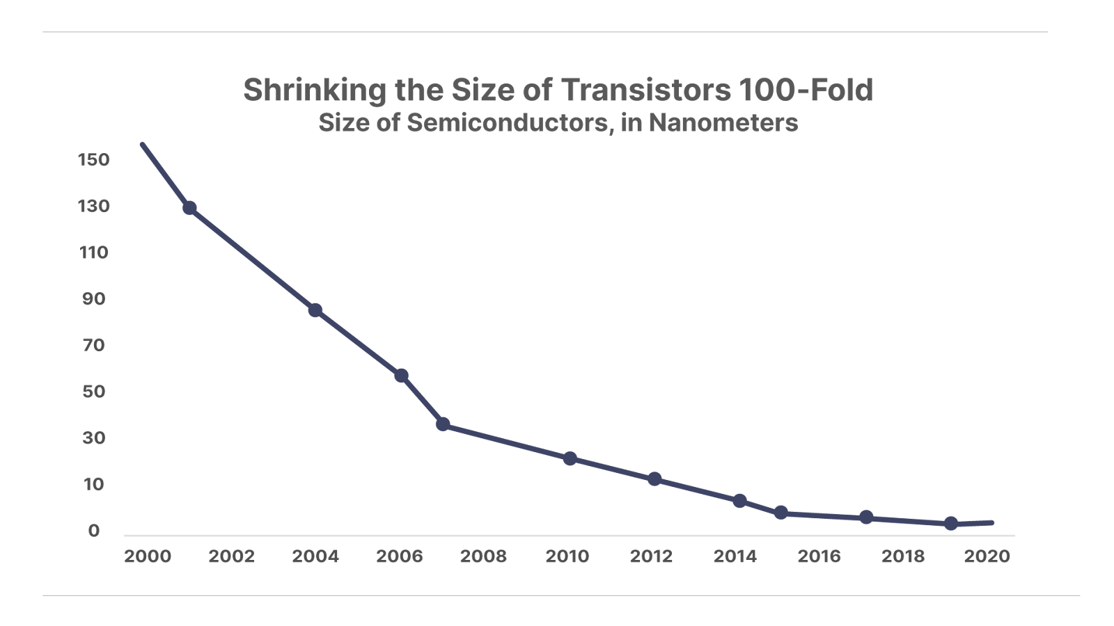
The latest class of sub-10 nm semiconductors powers today’s parallel-processing revolution. It’s how Nvidia designed its latest Blackwell B100 GPU with an incredible 208 billion transistors packed into a single chip – the most of any GPU chip in the world. A GPU, as we discussed in detail last week, is a graphics processing unit – a specialized computer processor originally designed to speed up graphics rendering in video games.
ASML’s lithography machines are the only devices in the world capable of manufacturing the sub-10 nm chips powering Nvidia GPUs, along with every other high-end computer chip on the market. The story of how it got here provides the key context for understanding why ASML will remain a monopoly for years to come.
Early Success Stalled by a Technological Wall
When ASML first entered the lithography market in 1985, it was a small fish in a big pond. Japanese firms like Canon and Nikon dominated the industry, and ASML struggled to compete against these larger and more established rivals.
ASML’s first breakthrough came in 1991, with the release of its cutting-edge PAS 5500 lithography machine. ASML struck a long-term deal to supply the PAS 5500 for Micron Technology, at the time one of the world’s largest memory and storage chipmakers. The deal turned ASML from a struggling upstart into a respected name in the industry. The deal also transformed ASML’s financials from showing consistent net losses to generating over $100 million in net income every year by the mid-1990s. The company reinvested heavily into research and development (R&D) to launch a series of newer, more advanced machines throughout the decade.
Lithography machine makers like ASML have two primary modes of innovation for etching ever-smaller transistor sizes onto silicon wafers.
The first comes from tapping into new sources of lower-wavelength light energy. Think of shorter wavelength light as providing a thinner paint brush to imprint finer details onto a canvas – or silicon wafers in the case of chip making. When the first semiconductors were created in the 1960s, lithography devices used visible light in the 435 nm spectrum. From there, the industry progressed toward ultraviolet light, in the 365 nm spectrum, and then deep ultraviolet systems, at 193 nm, by the 1990s.
The second key innovation for shrinking light wavelengths comes from advancements in optical systems. Lithography machine makers use complex optics systems containing a series of lenses to focus and reduce the source light down to even-thinner wavelengths.
Throughout the 1990s, ASML rose to the forefront of the industry by implementing cutting-edge optics systems, first tapping into ultraviolet light in the 365 nm range then using advanced lasers for tapping into the 193 nm range.
However, by the late 1990s, ASML and other lithography leaders ran into a technological wall. The industry had exhausted its ability to harness shorter wavelengths of light energy, and advancements in optics could only go so far in shaving deep ultraviolet light down to fewer nanometers of functional wavelengths.
The next step involved crossing a major chasm into extreme ultraviolet light (“EUV”). This promised to shrink the silicon-board paint brush by 90% from the 193 nm wavelengths in the deep ultraviolet spectrum down to 13.5 nm of EUV light. But tapping into this new frontier presented massive technical challenges that defeated virtually every company that attempted it.
Crossing the EUV Chasm With Help From Uncle Sam
The first major obstacle to unlocking EUV lithography technology was producing a 13.5 nm source light. At the time, no commercial laser system existed for reliably producing EUV light at the demanding levels of precision required in lithography machines.
Another major complication was the fact that EUV light is absorbed by glass and air. This meant the traditional industry approach of using glass lenses to focus the light beams was not workable. Instead, engineers would need to use mirrors to direct the EUV light beam onto silicon wafers. But the 13.5 nm wavelength of EUV light is so small that the existing mirrors available wouldn’t reflect it. Afinal challenge was that the whole thing needed to operate within the confines of a sealed vacuum chamber, to eliminate interaction with ambient air (which is air in its natural state, which would absorb the EUV energy).
The scientific and engineering hurdles were so daunting that two of the leading lithography companies of the day, Canon and Nikon, gave up on EUV technology in the 1990s. By this point, many considered the development of EUV lithography to be impossible. Some even predicted that the stalled progress in lithography advancement would mean the end of Moore’s Law.
In 1997, the U.S. government stepped in to help the industry solve the daunting technological challenges of EUV lithography. The Department of Energy (“DoE”) funded a six-year EUV research program, managed through a public-private partnership between top university laboratories and industry leaders. The U.S. government retained control over any technology developed through the partnership, which it owned though an entity called the Extreme Ultraviolet Limited Liability Company (EUV LLC). This meant that any company that wanted to use the technology developed by EUV LLC would first need to get approval from the U.S. Congress.
The EUV LLC initiative achieved numerous technological milestones that would later lead to the development of the first commercial EUV lithography machines. But the U.S. government was very selective in granting licenses to this critical technology. Specifically, the DoE denied access to Nikon and Canon.
One of the companies that participated in the EUV LLC initiative, and thus gained access to the technology license, was Silicon Valley Group (“SVG”). SVG was a U.S. lithography equipment maker based in San Jose, California, that ASML acquired in 2000 (and for a strategic reason we will explain later), giving ASML ownership of the technology license. Over the next six years, the company invested heavily into advancing the learnings from EUV LLC. Then in 2006, ASML unveiled the world’s first working prototype of an EUV photolithography machine.
But producing a successful prototype was only the beginning of a long slog toward commercializing the technology. It took ASML another seven years – and billions more in R&D – to produce the world’s first commercially available EUV lithography machines. Fast forward more than a decade, and ASML is the only company in the world that has developed usable EUV lithography.
To understand why this technology required such a painstakingly long development period, let’s explore what have been called “the most sophisticated machines ever manufactured.”
Small Transistors, Giant Machines
ASML’s latest product iteration, released in 2023, is called a High-NA-EUV lithography machine. The High-NA stands for high numerical aperture, which describes the cutting-edge optics system used to shrink EUV light down to an 8 nm wavelength. This reflects a 1.7x improvement from ASML’s original 13.5 nm EUV lithography machines, first released in 2013.
Creating these nano-sized light wavelengths requires a massive machine containing over 100,000 parts and weighing 165 tons – the equivalent heft of two commercial jet airplanes. When ASML shipped its first High-NA-EUV machine to an Intel factory in Oregon last December, the parts alone filled the cargo holds of four 747s. And once the parts arrived, it took 250 engineers six months to install the mammoth machine (pictured below).
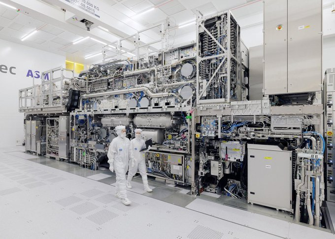
Properly describing the intricacy of these machines would require a full-length dissertation.
For a brief bit of insight, consider what goes into the production of the EUV source light alone. ASML, working with its key suppliers, had to create one of the most sophisticated laser systems in the world to generate this light source.
The process begins with a device that shoots tiny droplets of molten tin (25 microns in diameter, or about a third of the width of a human hair) through the air at 230 feet per second. As the drops fall, a laser beam strikes the tin molecule at precisely the right angle to flatten it into the intended shape. Next, a second laser beam vaporizes the tin into a superheated plasma, reaching a temperature of 220,000 degrees Celsius (40 times hotter than the sun) to generate the EUV light. The process is repeated 50,000 times each second, requiring unimaginable levels of speed and precision. The calculations used to zap the tin molecules in mid-air involve more precision than those used to navigate the Apollo lunar module to the moon.
Once the EUV light is created, it must be directed toward precise, nano-sized targets on the silicon wafer through a complex mirror system. The EUV light wavelength is so small that typical high-tech mirrors won’t reflect it. So ASML had to work with its key optics supplier – German company Zeiss – to create a custom-designed mirror just for ASML machines. The manufacturing process uses a high-precision ion beam that shaves the mirror surface one individual molecule at a time, making it what ASML calls “the most precise mirror in the world.”
The diagram below shows the complex gauntlet of mirrors the machine uses to direct EUV light onto a silicon board, etching out patterns within a quarter of a nanometer’s precision (about the width of an individual atom):
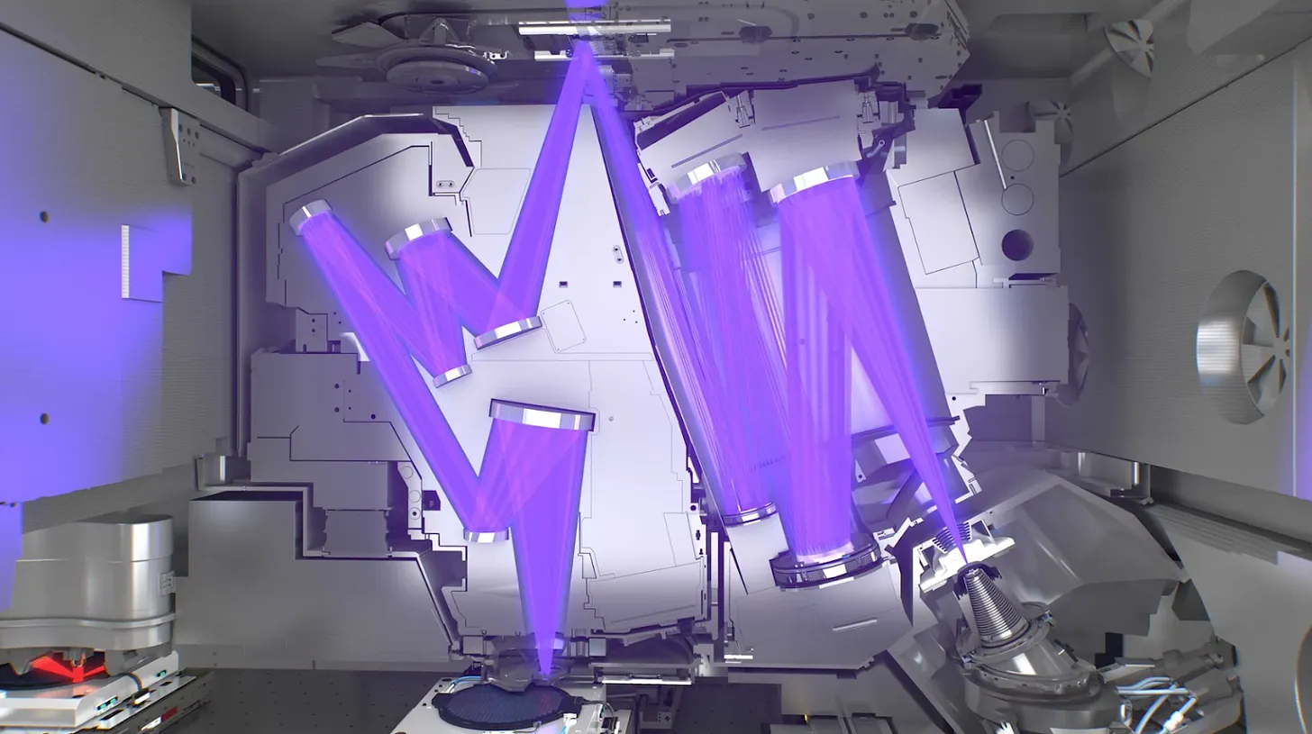
This is just one aspect of the complexity that goes into ASML’s machines that etch the intricate patterns in today’s most advanced 2 nm to 3 nm semiconductor chips.
Overruling Moore’s Law
While companies like Nvidia (NVDA) deserve much of the credit for engineering today’s cutting-edge sub-10 nm chips, they would be impossible to manufacture without ASML.
Leading tech publication MIT Technology Review has heralded ASML’s EUV lithography equipment as “the machine that saved Moore’s Law.”
To be clear, ASML’s ongoing advancements in EUV lithography saved the idea of Moore’s Law and its notion of measuring constant improvements in processing speed. But the original Moore’s Law computation has been left in the dust.
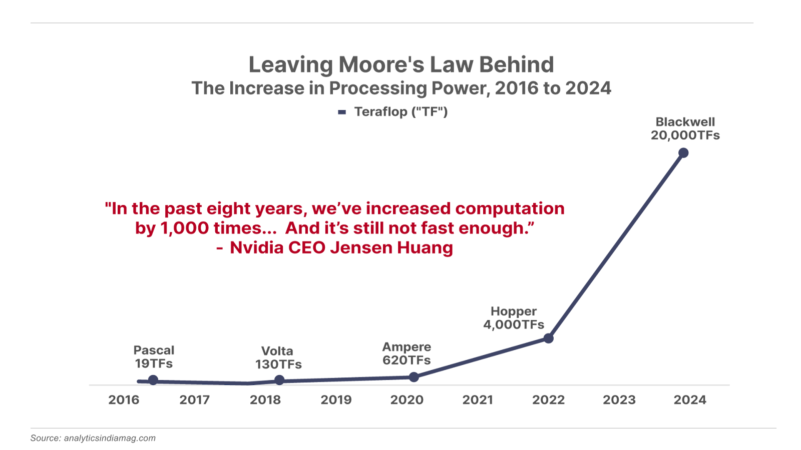
Consider the trajectory of computing power in Nvidia’s cutting edge GPU chips in recent years. The standard measure of computational capacity is a term known as “floating point operations per second” (“FLOPS”), which refers to the number of arithmetic calculations a chip can perform per second. The power of today’s most advanced chips are measured in Teraflops (“TF”), where one TF equals one trillion FLOPS.
In just the last eight years, the computational capacity of Nvidia’s GPU chips, all of which are manufactured by ASML machines, have increased 1000-fold from 19 TFs to 20,000 TFs. That’s four times the 256x rate of increase suggested by Moore’s Law over the same period:
Today, ASML controls 90% of the global market share for all lithography machines used in semiconductor manufacturing. But most importantly, it sells 100% of the EUV lithography machines used to make sub-10 nm semiconductors. The demand for these chips goes beyond Nvidia GPUs and the AI arms race. These semiconductors power all of the latest generation of electronics used in consumer devices (smartphones, tablets, and PCs), industrial applications (data centers and 5G telecommunication networks), and in the military (drones, fighter jets, and missile guidance systems).
So while ASML is one of the biggest beneficiaries from the rise of parallel computing, its revenue stream is far more resilient than most other companies riding this boom. Given its monopoly position as the sole lithography supplier to high-end chipmakers across every end market, ASML enjoys a steady source of new demand from the rising tide of semiconductor manufacturing across the board.
That’s how the company has increased its revenue over the last decade at a compounded annual growth rate (“CAGR”) of 17%, regardless of the booms and busts in different chip segments (i.e., crypto mining, metaverse, and now AI and parallel computing):
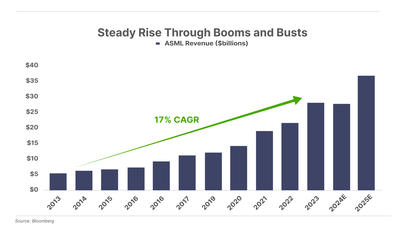
There’s one key factor that instills great confidence in ASML’s future growth prospects, regardless of which companies win the AI arms race, or how the trends in semiconductor technology evolves. That one key factor is its virtually impenetrable competitive moat that continues growing wider.
A Dominant and Growing Competitive Moat
When ASML first entered the lithography market, it was playing from a position of weakness against the industry giants Nikon and Canon. Even after ASML introduced a line of successful products in the mid-1990s, the two companies together generated 10 times the earnings of ASML. But since commercializing EUV lithography, ASML has produced a growing stream of profits that it has continuously recycled into R&D. Today, as the world’s dominant supplier of lithography machines, ASML generates four times as much income as those top two rivals combined:
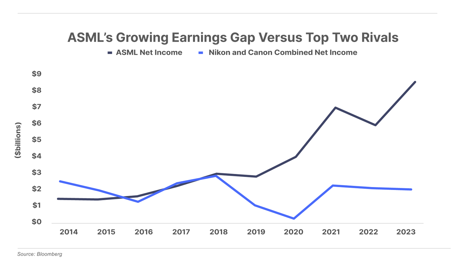
ASML is now playing from a position of incredible strength. Its unmatched earnings power gives it the ability to pour $1 billion a quarter into R&D, or double what its next closest competitor, Nikon, invests. That’s how the company continues introducing cutting-edge EUV lithography machines, while the rest of the industry struggles to even gain a foothold into the market.
But ASML’s R&D spending is only the first layer of its competitive moat. Even when companies with bigger R&D budgets have attempted to enter the market, they’ve failed.
This most notable example is Intel – one of the world’s largest chipmakers – that tried mastering EUV lithography for its own semiconductor manufacturing lines in 2012. At the time, Intel’s $5 billion R&D budget dwarfed the $600 million ASML invested each year into R&D. In 2012, Intel announced a $4 billion commitment to developing its own EUV lithography machines.
Intel was part of the original consortium of private companies that partnered with the U.S. Department of Energy as part of the EUV LLC initiative in the 1990s. This meant Intel had access to the same technological starting point as ASML, and a significantly larger budget.
And yet, Intel gave up on its EUV program. Today, Intel is now a customer of ASML – paying ASML $380 million for just one High-NA-EUV machine last year.
Even the Chinese company Dongfang, created in 2014 by Zongchang Yu – the former ASML engineer who orchestrated the theft of all 2 million lines of source code used in ASML’s EUV lithography machines – has failed to produce a commercially viable EUV system. And that’s despite the backing of the Chinese government.
Thus, the question at hand: why have no other companies successfully replicated ASML’s EUV technology – even well-financed competitors working with bigger R&D budgets and similar technological starting points and those using an exact copy of ASML’s stolen intellectual property?
ASML’s Big Secret: A Dominant Supply Chain
ASML has done far more than master an incredibly hard-to-implement technology by itself. The company has amassed a complex supplier network spanning over 5,000 companies that work hand-in-hand with ASML to produce the more than 100,000 components in each EUV machine. Many of these suppliers are highly-specialized equipment makers that are themselves monopoly providers of equipment. In some cases, ASML has exclusive partnerships that prohibit doing business with the competition.
Consider the case of optics maker Zeiss. Zeiss, as mentioned earlier, worked with ASML to develop the custom mirrors capable of reflecting EUV light. ASML has maintained a long-running partnership with Zeiss. The relationship frayed in the late 1990s when ASML discovered that Zeiss was selling optics equipment to competitor SVG. ASML responded by acquiring SVG and locking in an exclusive relationship with Zeiss. In 2016, ASML took a 25% equity stake in Zeiss, and as part of the deal, gave Zeiss CEO Peter Grassmann a seat on ASML’s board. Today, ASML refers to the relationship as “two companies, one business.”
When ASML can’t control suppliers, or when quality standards disappoint, it simply buys them. Author Chris Miller describes these aggressive tactics in his best-selling book Chip War: The Fight for the World’s Critical Technology. Miller explains that Peter Wennink, who served as ASML’s CEO from 2013 – 2024, has been known to warn suppliers: “If you don’t behave, we’re going to buy you.”
One high-profile purchase by ASML was of EUV-light-source manufacturer Cymer, for $2.5 billion in 2012. That was the same year Intel announced its $4 billion commitment to develop its own EUV lithography system. Cymer’s laser technology was considered so critical to EUV development that an industry analyst with investment bank RBC Capital Markets noted at the time: “This is a one-of-a-kind deal… EUV is pretty much down to ASML.”
And therein lies the big secret to ASML’s iron grip on EUV lithography. With more than 100,000 parts needed to manufacture these systems, no one company can do it all on its own. ASML has a stronghold on the key choke points of the supply chain needed to produce these machines. This includes a tight strategic relationship with Zeiss, the only optics company capable of making the mirrors that reflect EUV wavelength light. And through its acquisition of Cymer in 2012, ASML owns the only company that can produce critical components for EUV light-source generation.
These are just two examples that illustrate the key point: replicating ASML’s success in EUV lithography machines requires much more than a giant R&D budget, or simply stealing the intellectual property.
An analogy would be a time traveler going back to the 1700s and dropping off the blueprints for a Ford F-150 pickup. Even if a person from that era could decipher the diagrams, they’d have no way of securing the machined metal and other parts needed to build the vehicle. Without a vast network of component suppliers, the blueprints would be worthless.
The same is true for ASML’s competitors. Any new entrant into this market would need to painstakingly replicate ASML’s 5,000-plus network of key suppliers. But ASML has already taken many of the critical players in this supply chain off the market, either through acquisitions or exclusive partnerships.
There’s one final aspect of ASML’s business that’s hard to replicate: the ongoing service and support required to maintain the company’s complex machines. Each lithography machine that ASML ships comes with a full-time support staff of technical experts that remain onsite for the full length of the machine’s life (typically around 20 years). These technicians do everything from routine maintenance to replacing broken parts, as well as continuously fine-tuning the precision machine for optimal performance.
Training a workforce with the high-tech skills needed to provide this support only comes with years of hands-on experience working directly with these machines – a process that would take years to develop, even after a competitor successfully mastered EUV lithography technology.
Another advantage of this service – it provides ASML with a steady source of recurring revenue, which has historically made up between 20% to 30% of its business. This creates a high degree of stability in ASML’s business, by providing a source of ongoing returns from each machine for up to 20 years after the original sale. And this high level of service is critical for ASML’s customers, by ensuring they maximize the performance and run-time out of each machine they buy. Any new competitor hoping to enter the market would have to replicate this critical service feature of the business.
When viewed through this lens, it’s easy to see how ASML has established a monopoly position in EUV lithography machines. Through its acquisition of SVG in 2000, it secured an early advantage over its two key rivals, Nikon and Canon, by tapping into the exclusive technology developed by the EUV LLC public-private partnership. From there, it poured billions into advancing the technology and developing the first working prototype in 2006.
By the time other competitive threats emerged, including Intel in 2012, ASML had secured major choke points of the supply chain required to produce these incredibly complex machines. This has made it virtually impossible for its competitors to enter the market, allowing ASML to further extend its advantages in technology, supply-chain dominance, and service. From this leading position,it’s very difficult to imagine a scenario where a competitor displaces ASML.
The Ultimate Forever Stock
ASML’s dominant competitive position as the sole supplier of EUV lithography machines makes it the ultimate “forever stock.” Its competitive position has been secured through 30 years of R&D investment and the cultivation of its intricate supplier network.
The company’s products will remain in high demand so long as the world continues requiring higher volumes of advanced sub-10 nm semiconductors. This is a trend that will likely continue indefinitely, regardless of which companies and technologies rise and fall along the way.
ASML’s monopoly position ensures a long runway of growth, and also gives it incredible pricing power. Nowhere is this more evident than in the hefty $380 million price tag of its latest High-NA-EUV machines.
At a May technology symposium in Amsterdam, a senior executive at Taiwan Semiconductor (“TSMC”) – the world’s leading manufacturer of sub-10 nm semiconductor chips – noted:
“I like the High-NA EUV’s capability, but I don’t like the sticker price.”
The comment did not reflect a deal-breaking concern, however. One month later, on June 5, it was announced that TSMC had placed an order for the $380 million machine.
One industry analyst summed the current reality: “You can’t make leading-edge chips without ASML’s machines.”
Any chipmaker that doesn’t want to get left behind in the never-ending race toward greater computing power has no choice: ASML is the only game in town.
ASML is the only company that can supply the critical lithography machines needed to make today’s sub-10 nm computing chips. The parallel computing revolution and AI arms race will likely fuel a surge in demand for these machines in the coming years. Analysts currently expect the company will generate $39 billion in revenue next year, up nearly 40% from 2023. Meanwhile, ASML’s profit margins are expected to increase to 32%, up from 28% last year, as it benefits from growing sales of its latest $380 million High-NA-EUV machines. This translates into a 2025 earnings per share estimate of $32.
At the current price of $1,053, ASML shares trade at a forward price-to-earnings multiple of just under 33x. Given its monopoly position as the sole supplier of machines needed to make the semiconductors that power the global economy, with a long runway of highly-profitable growth ahead, we believe this is a reasonable – though not cheap – price to pay for ASML shares.
While its valuation is arguably justified at current levels, we believe there will come a time when the shares offer a “no-risk” entry price – which they do not at the moment. This could come from any number of factors including a short-term production glitch, a slowing global economy, or financial market volatility.
For now, we’re putting ASML on our watchlist, to buy when shares become more affordable. In the meantime, stay tuned for future updates.
The next company that’s positioned to become one of the inevitable winners from today’s parallel-computing revolution is a business that, like ASML, has secured a dominant and irreplaceable place in the global semiconductor supply chain.
The World’s Most Important Company
Taiwan Semiconductor Manufacturing (NYSE: TSM) is the world’s largest semiconductor manufacturer. While TSM isn’t a monopoly in its market like ASML, it’s a close second – it produces 90% of the world’s most advanced sub-10 nm computing chips.
However, TSM is arguably the most fragile link in the global semiconductor supply chain, because China views the self-ruled island nation of Taiwan as a breakaway province. The Communist Chinese government believes it and the 24 million people who live there will eventually be reunified with mainland China, under the threat of force if necessary. Adding to the uneasiness is the fact that the U.S. has vowed to support Taiwan’s claim to independence.
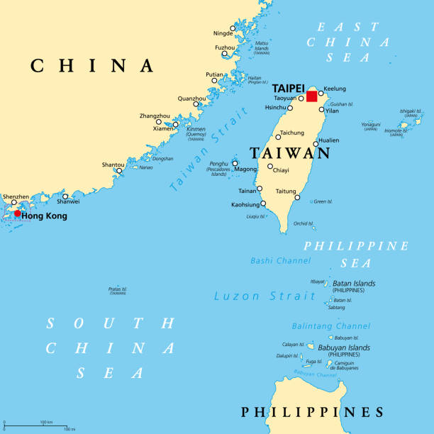
This has created a tense war of words between the U.S. and China over Taiwan’s fate as a sovereign nation. A geopolitical showdown over the small island country would have devastating consequences for the world’s supply of today’s most critical resource: advanced semiconductors.
Bloomberg estimates that a war over Taiwan could cause a $10 trillion hit to the global economy – five times the $2 trillion in losses from the Great Financial Crisis.
Fully appreciating the critical role TSM plays in the global economy starts with understanding why companies like Nvidia, featured in last week’s Big Secret issue, and virtually all other leading semiconductor companies, don’t actually manufacture the chips they sell. Instead, they create the blueprints, and submit those designs to contract manufacturers, like Taiwan Semiconductor.
This outsourcing model made good financial sense when it first emerged in the 1980s. Back then, there were dozens of contract manufacturers, and no one company held a dominant role in the industry.
But as we’ll explain here, TSM perfected this outsourcing model better than anyone else over the course of nearly four decades. It’s risen from a second-rate manufacturer of low-margin, commoditized chips to the most dominant semiconductor maker in the world – by a wide margin.
With control over 90% of the supply of advanced semiconductors, TSM represents a bigger geopolitical choke point – on a product that’s arguably more important to the global economy than oil – than all of OPEC, which controls just 40% of the global oil supply.
The story of how the world’s chip supply became dominated by one company all begins with a high-ranking executive that was passed over for a promotion in 1985.
Trial and Error and Lower Costs
By all rights, Morris Chang was a lock to become the next CEO of Texas Instruments (“TI”), America’s leading chipmaker, in the mid-1980s.
After immigrating to the U.S. from China and earning a degree in mechanical engineering from MIT, Chang joined TI in 1958. At the time, TI was at the cutting edge of developing the new class of silicon-based semiconductor chips.
Chang proved himself as a brilliant engineer and problem solver early on at TI. In one of his first major assignments, he was tasked with solving one of the company’s biggest challenges: fulfilling a contract TI had with IBM to help the computer company manufacture its first silicon-based chips for mainframes.
IBM had problems manufacturing the chips in-house, achieving production yields of just 10% (meaning 90% of the chips produced were thrown away). When TI began producing the same chips for IBM, its yields were even worse. Within four months of taking over, Chang achieved a 20% production yield – or twice as good as what IBM had been able to do.
Chang proved himself as a brilliant businessman as well. By 1967, he had become general manager of TI’s burgeoning semiconductor business. In this role, Chang made a key breakthrough that would ultimately set the stage for TSM’s dominant business model today.
Chang realized that the biggest economic force governing chipmaking was scale. Chipmaking facilities aren’t the typical, commoditized factories that anyone can build. They require immense precision, cutting-edge technology, and – most importantly – trial and error to get yields up (as Chang had done with the IBM chip line). None of this comes cheap.
In the 1960s, industry practice was to pass all of these upfront trial-and-error costs onto the customer. This meant charging high initial prices on new chips, with the aim of reducing prices after recouping their initial investment.
But this presented a catch-22. The high initial prices meant the buyers of chips couldn’t afford to order in bulk. Thus, chipmakers might get the prices they wanted, but not in the volume they needed. This meant chipmakers had to run their plants below capacity, resulting in bloated overhead costs that limited their overall returns.
Chang hired Boston Consulting Group (“BCG”) to conduct a wide-ranging study on the economics of chipmaking. Chang and BCG came up with a concept called “learning-curve pricing.” This was a controversial strategy that involved charging low prices from the beginning, and then consistently reducing prices more – even when the market did not demand it.
Many in the industry thought this was a crazy strategy. And in the short run, they were right. It was very expensive, requiring TI to operate at a loss in the early phase of ramping up new production lines. But Chang had a long-term vision. By cutting prices aggressively, TI was able to secure more business, overcoming the volume hurdles that plagued the traditional industry approach.
By aggressively lowering prices, TI successfully pulled business away from its higher-cost competitors. This strategy turned TI into the industry’s largest semiconductor manufacturer. And with all of this volume, TI could spread its fixed costs over a larger number of units, also making it the most profitable chipmaker in the world.
By the late 1970s, Chang’s learning-curve pricing strategy had helped TI achieve the critical economies of scale required for profitable semiconductor manufacturing. Chang (along with pretty much everyone else at TI) expected he could eventually become CEO.
But in 1985, for reasons still unclear today, Chang was passed over for promotion to the Texas Instruments CEO role. Chang resigned in frustration. This ultimately created the catalyst for him to accept an invitation to take his talents to the small island country of Taiwan, just off the coast of mainland China, where he used his learnings from TI to upend the global order in semiconductors.
A Chip Manufacturing Giant Is Born
In the 1980s, Li Kwoh-ting (today known as the “father of Taiwan’s economic miracle”) had a grand vision to transform the country into a global tech giant. In 1987, the economist and political leader recruited Morris Chang to become CEO of a new public-private partnership called Taiwan Semiconductor Manufacturing Company. The goal was to make TSM into the preeminent manufacturer of semiconductor chips.
At the time, Taiwan had no expertise in chipmaking, or any other advanced technology for that matter. The country’s manufacturing base centered around low-margin, commoditized products.
What Taiwan did have was a vast supply of cheap labor. This was enough to get TSM started by mass producing the low-margin, older-generation chips that other companies didn’t want to make. While TSM’s early profits were slim, Chang had learned from his TI experience that long-run value came with greater economies of scale. So he aggressively reinvested into R&D, advanced manufacturing equipment, and on-the-job training for TSM’s workforce.
By the mid-1990s, TSM’s manufacturing capabilities began closing the gap with some of the world’s most advanced chipmakers. And the timing couldn’t have been better. Under growing pressure from overseas competitors, U.S. chipmakers began outsourcing production of even their most-cutting-edge semiconductors – opening up a massive source of new and increasingly profitable business for TSM.
Japanese Competition Forces U.S. Chipmakers Into Outsourcing
When the semiconductor industry emerged in America in the 1960s, most chipmakers were fully vertically integrated – meaning they controlled everything from design to manufacturing. When they did outsource production, it was limited to their lower-margin chips.
However, fierce competition from Japanese chipmakers changed everything, starting in the 1970s and accelerating throughout the 1980s. Japanese manufacturers gained an edge with the help of the Japanese government, which provided large tax incentives and funding programs to spur R&D. As a result, total semiconductor R&D went from 2% of Japan’s industry total in the early 1970s to 26% by 1977.
By the 1980s, Japanese chipmakers began dominating the market for products like VCRs, which at the time contained the most semiconductors of any consumer device. They also introduced new cutting-edge consumer technology, like the Sony Walkman, a portable music player that was the precursor to Apple’s iPod.
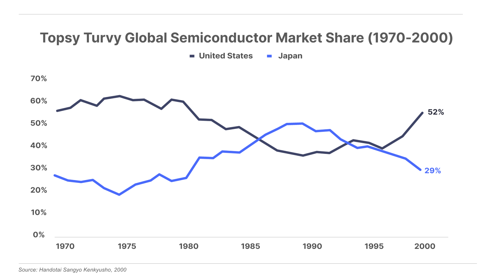
By 1986, Japan overtook America as the dominant force in semiconductor manufacturing, with over 50% of the global market share. As a result, U.S. chipmakers had less money to invest into R&D, putting them even further behind, and creating a self-reinforcing downward spiral.
One by one, U.S. chipmakers realized they had only one good option to regain their competitive foothold: outsource manufacturing. This concept gave rise to what we now call the “fabless” semiconductor model. In this model, semiconductor companies focus entirely on researching and designing cutting-edge chips and then sending those blueprints to third parties for mass production – either to other vertically-integrated chip makers with excess production capacity, or to “foundries” that focused exclusively on manufacturing for other companies, but not designing their own chips. In this way, chipmakers still retained the high profit margins from selling cutting-edge semiconductors, while eliminating the huge capital requirements of running a foundry.
For the old guard who grew up in the vertically integrated model, outsourcing production was anathema to their DNA. Jerry Sanders, the flamboyant founder and CEO of Advanced Micron Devices (“AMD”) during the 1980s, famously declared that “Real men have fabs,” in a less-than-subtle jab at his outsourcing competitors.
But the financial force of capital efficiency couldn’t be ignored. By the mid-1990s, a growing number of U.S. chipmakers began adopting the fabless model. Over time, this freed up their capital to invest more into R&D, enabling America’s top chipmakers to regain their competitive lead designing the world’s most innovative chips – without manufacturing anything themselves.
So even as America’s share of chip manufacturing dropped to an all-time low by the end of the 1990s, its share of total chip sales rose above 50% – recovering from a drop below 40% in the 1980s. Meanwhile, Japanese chipmakers fell by the wayside, entering the new millennium with just 29% global market share:
TSM found itself perfectly positioned during this 1990s outsourcing boom.
The company enjoyed a couple of key advantages as the world’s first – and for a long time, the only – pure-play semiconductor manufacturer. Before TSM, the only outsourcing options involved partnering with a fully-integrated chipmaker that would effectively rent out their excess production capacity.
This model created inherent conflicts of interest, given that the manufacturer was often in competition with its customers. And once a company learns how to produce a competitor’s chips, it’s not a giant leap for that company to find ways of mimicking that design.
The brilliance of Chang’s approach at TSM was to build a company that purposefully avoided competing with its customers.
TSM’s business model was particularly appealing to new startups, which often had valuable IP, but few resources to shield that IP from larger competitors. Thus, TSM became a go-to choice for many up-and-coming fabless chipmakers in the 1990s. One of these startups was a then-little company called Nvidia. Founded in 1993, Nvidia got off the ground with just $40,000 in the bank and $20 million in venture-capital financing. TSM was the key that enabled new entrants like this small California chip designer to enter the semiconductor market, without facing the daunting capital requirements of building its own production facilities.
TSM became Nvidia’s primary chip manufacturer in the mid-1990s, and the partnership has flourished ever since. As Nvidia rose to become one of the world’s most valuable companies, worth $3 trillion today, it brought TSM along for the ride.
And this long-running partnership underscores another major competitive advantage that sets TSM apart from the competition. The brilliance of TSM’s pure-play foundry model meant that the company’s fortunes were never tied to any single chip architecture. Instead, TSM’s manufacturing capacity followed the demand trends from its most successful customers, like Nvidia, Apple, and Qualcomm.
And it’s paid off handsomely. Since going public in 1994, the company has grown its revenue at a CAGR of 18%. Over this 30-year stretch, TSM has only posted three years of revenue declines – each caused by broader macroeconomic slowdowns. These include the 2001 dot-com bust, the 2008 Great Financial Crisis, and the 2023 post-pandemic slump in smartphone and PC demand. Revenue is on track to rebound to new highs this year from the booming demand for AI chips:
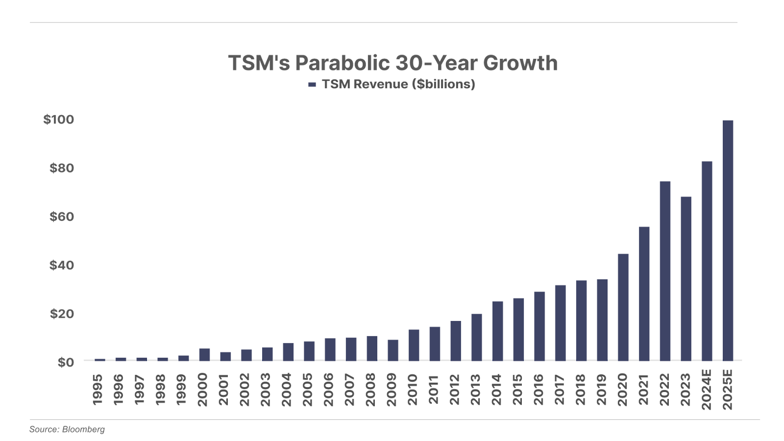
Along the way, TSM aggressively reinvested its growing revenue stream into advancing its production capabilities.
So while TSM started off as a low-margin producer of older-generation chips in the 1980s, everything changed when the outsourcing boom took hold in the 1990s. By the early 2000s, TSM had advanced its capabilities to become one of just 31 companies in the world capable of producing the most advanced 150-nm chips of the day.
Over time, the number of semiconductor manufacturers capable of producing the most advanced chips began dropping off. Part of this was a result of the ongoing trend of outsourcing. Even longtime holdout AMD relented and spun off its manufacturing operation into its own business, GlobalFoundries, in 2009.
And for the companies that continued to both design and make their chips, their foundries were tied in with whatever chip architecture they specialized in. Good or bad, they had to continue producing the chips they designed. As technological trends shifted, many of these companies became cut out from the leading edge of semiconductor manufacturing.
Since TSM had no allegiance to any single chip architecture, it continued grabbing more market share as other foundries fell by the wayside. The never-ending disruptive force of technological evolution became a perpetual boon to TSM, while gradually eliminating other top foundries. As a result, the market for cutting-edge chip manufacturing naturally accrued to TSM.
From 2000 to 2020, the number of companies capable of producing the world’s most advanced semiconductor chips fell by 90% from 31 down to just three:
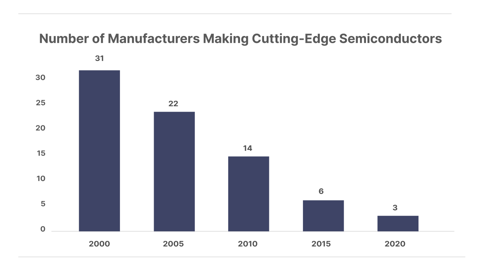
Of those three, TSM is number one. Today, it is the dominant global manufacturer of advanced sub-10 nm chips, with over 90% market share. The other two companies vying for second best include the U.S.-based Intel and Korea’s Samsung.
Samsung and Intel are both vertically-integrated manufacturers that primarily make chips for their own product lines. They both offer foundry services for other chipmakers, but this is a minor subsegment of their overall businesses. Moreover, Intel and Samsung both face the same constraint discussed earlier: they often compete head-to-head with their foundry customers.
TSM, on the other hand, is in a league of its own. It’s the world’s only pure-play foundry with sub-10 nm production capacity that dedicates 100% of its focus to supplying customers, rather than competing against them with its own designs.
Thus, for many of the world’s largest fabless semiconductor companies, TSM is the only game in town. It has secured long-standing partnerships to supply advanced chips for virtually all of the world’s largest semiconductor companies. Its key customers include Apple, Nvidia, Qualcomm, Broadcom, and AMD.
TSM enables these companies to generate enviable returns on capital, by handling the capital-intensive business of manufacturing the chips these tech giants design. Every year, TSM spends $30 billion on capital expenditures – or roughly double that of the five largest fabless chip makers combined:
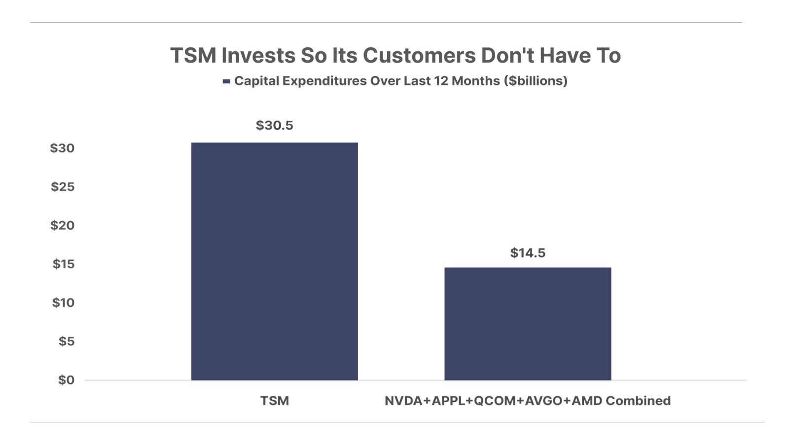
Aside from Intel and Samsung, no other company in the world invests in semiconductor manufacturing capacity at the scale of TSM. And that’s one of its most powerful competitive advantages today.
In order for any company to displace TSM’s dominant market position, it would first need to invest tens of billions of dollars into state-of-the-art production facilities. But that’s only the start. They would also have to spend many years mastering the art and science of optimizing their production yields.
TSM’s semiconductor plants are some of the most precise manufacturing operations on the planet. The sub-10-nm patterns TSM etches into silicon wafers are so intricate that a single speck of dust can ruin an entire batch of silicon wafers. This requires elaborate “cleanrooms” that are 10,000 times more sterile than the operating rooms in a modern-day hospital. Engineers must at all times work in protective suits, masks, and gloves. The air is so sterile and free of moisture that engineers must consume gallons of water each day to stay hydrated.
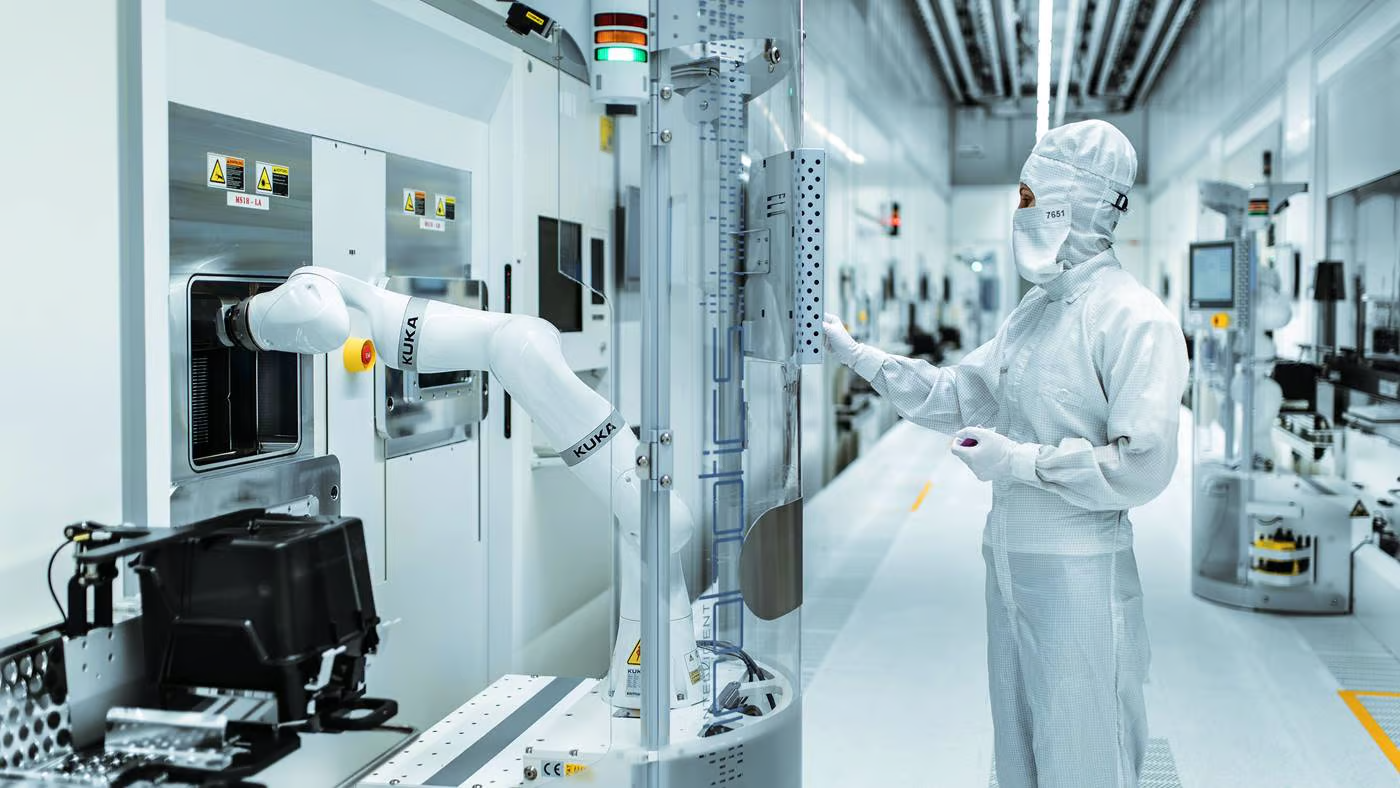
Despite the elaborate protections, speed is of utmost necessity. For that, TSM has installed some of the most sophisticated, high-speed robotics equipment in the world. From a mounted track in the ceiling of their plants, robotic shuttles transport chips through various stages of the assembly process, some of which are worth their weight in diamonds. The robotic shuttles in TSM’s plant travel a quarter-million miles each day, equal to 10 trips around the planet.
Recall from earlier, Morris Chang first rose to prominence at Texas Instruments by figuring out how to boost production yields up to 20% in the early 1960s, which was considered a good yield at the time. During the era of U.S. dominance in semiconductor manufacturing, the most efficient chipmakers achieved yields of 50%. When Japanese companies began displacing their American counterparts in the 1980s, they reached an average production yield of 60%. Today, Taiwan Semiconductor has reached 80% production yields – the best in the world. But it took many years of painstaking trial and error to get there.
As a Taiwan-based reporter for BBC recently explained, the “secret sauce” behind TSM’s manufacturing prowess is equal parts art and science:
Making microchips is engineering. But it’s also more than that. Some have likened it to cooking – like a gourmet feast. Give two chefs the same recipe and ingredients – the better cook will make the better dish.
Over its more than four-decade history, TSM has developed an irreplaceable body of institutional knowledge around chip making. By continuously tweaking its operating procedures through a never-ending series of trial and error, the company has perfected both the art and the science of chip making. While a competitor could try to replicate this process, it would take a herculean effort of time and human resources, and mountains of capital.
This presents a similar catch-22 situation that protects ASML’s secure position. In order to pull business away from TSM, a competitor would first need to replicate TSM’s incomparable scale and efficiency. Otherwise, a competitor could never compete effectively on price. But in order to match TSM’s scale and efficiency, a competitor would first need to attract enough business to justify the gargantuan investment in time and money.
The only viable solution would involve substantial external funding from a government. Even then, success is far from guaranteed. We’re seeing a real-world case study of this playing out in the U.S. today.
As we mentioned earlier, in 2022, the U.S. government passed the CHIPS Act, which authorized $52 billion in funding and tax incentives for the construction of new U.S. semiconductor manufacturing plants. This is part of the Biden administration’s efforts to reduce America’s reliance on Taiwan for today’s most advanced chips. Along those lines, the administration persuaded TSM to commit to building a $40 billion state-of-the-art plant in Arizona.
That $40 billion price tag would make it among the most costly manufacturing plants in the world, explaining why most chips are made overseas. America has become an expensive place to build large-scale manufacturing facilities. The price of land, materials, and (most important) labor is much higher compared with other key chip-making regions, like Korea and Taiwan. Consider that the $75,000 average household income in the U.S. is roughly five times that of the $16,000 in Taiwan.
TSM broke ground on the facility in December 2022, generating much fanfare about the coming resurgence of U.S. domestic semiconductor manufacturing. But the initial enthusiasm has now given way to a bleak reality.
TSM has struggled to recruit enough skilled workers even to complete the initial construction of the factory – getting significant pushback from labor unions. Meanwhile, TSM has also battled the endless red tape and bloated costs associated with the American bureaucratic machine. As Elon Musk recently explained, large-scale construction projects have effectively been made illegal in Western economies:
In the West, I think we have created regulatory gridlock where almost everything is illegal. This is why they can’t build a high-speed rail in California. They spent $7 billion and there’s a 1,600-foot section, it’s all they have to show for it and it doesn’t even have rails on it.
Production at TSM’s Arizona plant was originally slated to begin this year, but it’s since been delayed to 2025 because construction is not yet complete. Even when the factory comes online, many are skeptical that the plant will be able to compete on the global scale given the high costs of manufacturing in the U.S. One skeptic is a former TSM chairman, who described the Arizona chip plant as an “expensive, wasteful exercise in futility.” He also estimated that the U.S.-made chips will cost 50% more than those produced in Taiwan.
While the idea of a vibrant U.S. semiconductor manufacturing industry is appealing, we remain doubtful that the math will work – absent a radical overhaul in U.S. industrial policy. As California’s high-speed rail system shows, simply throwing money at the problem is not a solution. U.S. policymakers must dramatically reduce the bureaucratic burden on manufacturers to give them a chance on the global stage. But Washington isn’t even trying.
The bottom line: despite more than $50 billion in direct support from the U.S. government, plus tens of billions more from the private sector, all signs indicate TSM will retain its dominance over the global chip supply for years to come. The situation reminds us of Warren Buffett’s famous gut check for an enduring competitive moat, which he once described in reference to his favorite soft-drink maker, Coca-Cola (KO):
If you gave me $100 billion and said take away the soft drink leadership of Coca-Cola in the world, I’d give it back to you and say it can’t be done.
Like Coca-Cola, TSM’s wide competitive moat means even the most well-funded competitors can’t displace its dominant market position. As the only game in town for advanced semiconductor manufacturing, TSM commands premium pricing power for its chips. This is evident in the fact that the company makes more money on its chips than do its largest customers, most of which earn double-digit profit margins themselves. Generating an average of nearly 40% net income margins over the last three years, TSM is one of the most profitable companies in the world:
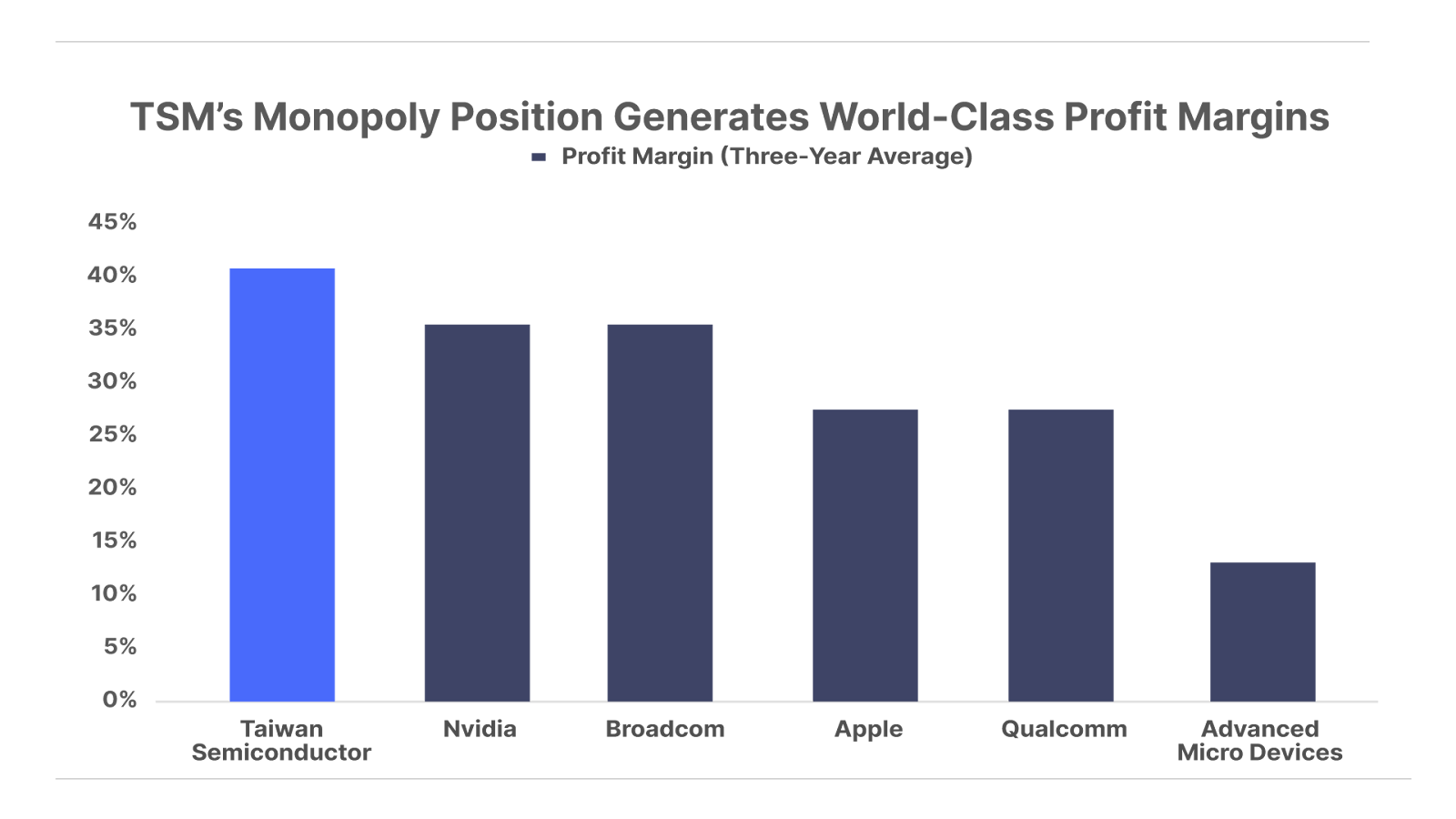
Despite the high capital requirements of its business, TSM’s monopoly-level pricing power generates returns on par with some of the world’s most capital efficient businesses. Over the last three years, TSM has averaged a 32% return on equity and 19% free cash flow margins. TSM shares have generated a compounded annual return of 22.5% since first going public on the Taiwan stock exchange in 1994.
Unlike many companies that run into the “law of large numbers” challenge to growth, TSM’s sheer size has become its most important competitive advantage. That’s how the company continues generating impressive growth rates, even though it’s already the world’s largest chipmaker.
Fueled by rising demand from today’s parallel-processing boom, analysts expect TSM will grow revenue 44% from $71 billion last year to $102 billion in 2025. Net income will increase 44% from $27 billion last year to $39 billion in 2025.
TSM currently trades at a market capitalization of $707 billion. Relative to the $39 billion it is expected to earn in 2025, that gives it a forward valuation multiple of just 18x price-to-earnings.
While this is a reasonable valuation based on forward earnings estimates, we’re not committing to a recommendation of TSM at this point. Despite our optimism about the long-term potential of the parallel-computing revolution, a growing body of evidence indicates that both the U.S. and global economy could enter a recession in the coming months.
A widespread slowdown in global growth will weigh on companies like TSM, which has historically experienced a revenue contraction during recessions.
As a result, we’re putting TSM on the watchlist. Stay tuned for future updates.
This content is only available for paid members.
If you are interested in joining Porter & Co. either click the button below now or call our Customer Care team at 888-610-8895.